IoT Interface Project
The Internet of Things (IoT) Interface Project is an effort to create a low-cost universal chip programmer which can also perform basic logic analysis, much like an oscilloscope. The project is to be created using an FPGA, opening the possibility for future development and features.
My name is Jacob Hazelbaker, a recent graduate of the University of Central Florida (UCF). In May of 2018 I completed my Computer Engineering degree at UCF, and I am now preparing to begin my graduate studies at Carnegie Mellon University within the Master of Science in Information Security (MSIS) program.
I am developing the IoT Interface Project under the guidance of two PhD students at UCF and Dr. Yier Jin of the University of Florida (UF). Dr. Yier Jin specializes in the security and trustworthiness of integrated circuits. http://jin.ece.ufl.edu/
With my time in the Distributed Research Experiences for Undergraduates (DREU) now complete, I have created a formal paper summarizing my work, which can be found here: IoT_Paper.pdf
Funding
Funding for the IoT Interface Project is made possible through the Distributed Research Experiences for Undergraduates (DREU) program. The DREU program was founded as a joint effort between the Computing Research Association Women (CRA-W) and the Coalition to Diversify Computing (CDC).
The National Science Foundation (NSF) provides funding for the DREU program, which I am delighted to be a part of for the Summer of 2018. Additional information about the DREU program can be found here: https://cra.org/cra-w/dreu/
Progress
Defining the Project
Throughout the first week my mentor, Dr. Yier Jin, and the PhD students at the Security in Silicon Lab (SSL) discussed with me various potential projects for me work on during the summer. My bachelor's degree is in Computer Engineering, which provided me some great opportunities to learn both the hardware and software aspects of computers. However, I am most passionate about computer security.
Therefore, the potential projects considered emphasized hardware and software development, as well as an opportunity gain additional experience with computer security. By the end of the first week, the IoT Interface Project had begun to take shape!
Early Hardware Diagrams and Learning LaTeX
It would seem that the majority of professional research papers are written in a scripting language known as "LaTeX", which is pronounced as LAY-tekh. I decided to gain some experience with LaTeX by creating a formal, 5 page summary of the various hardware diagrams I was considering for the project. The document can be found here: Update_2018_5_25.pdf
Identifying the Best Components for the Project
After deciding upon an overall hardware design for the IoT Interface Project, I set about identifying the best components to choose for project. The very challenging aspect was designing a system which could support a wide variety of programmable chips, varying greatly in form-factor and voltages used.
The primary component is an FPGA development board. At the conclusion of week 2 it was decided that the FPGA would implement the functionality of a logic analyzer and be capable of also performing many of the same functions as a Bus Pirate. The main function of the FPGA, however, is to serve as the primary component which would perform the universal chip programming.
After a very thorough search of various FPGA development kits, including all of the kits offered on DigiKey for under $300, I realized that the DE10-Nano kit featuring an Intel Cyclone V FPGA was the best choice for the project.
Planning How to Handle Various Chip Voltages and Currents
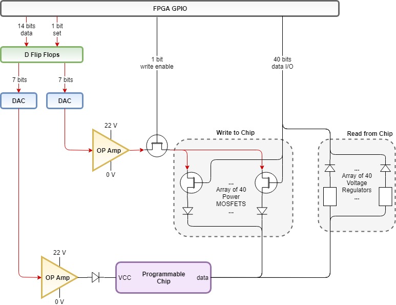
It became quite apparent that simply wiring up a chip to the GPIO pins of the FPGA might destroy the programmable chip, providing too much voltage and/or current to the chip. Moreover, some programmable chips require more voltage and current than the GPIO pins of the FPGA can provide.
I therefore set about designing an overall system design which could provide variable voltage and current supplies for the different types of programmable chips. The DE10-Nano dev board has an astonishing 40 GPIO pins, providing a great deal of flexibility in the design of this project. If I were instead using an FPGA with far less GPIO pins, then I might have to implement shift registers into the design of the external PCB.
The resulting, general design of the PCB to handle chip voltages and currents is displayed in the image below:
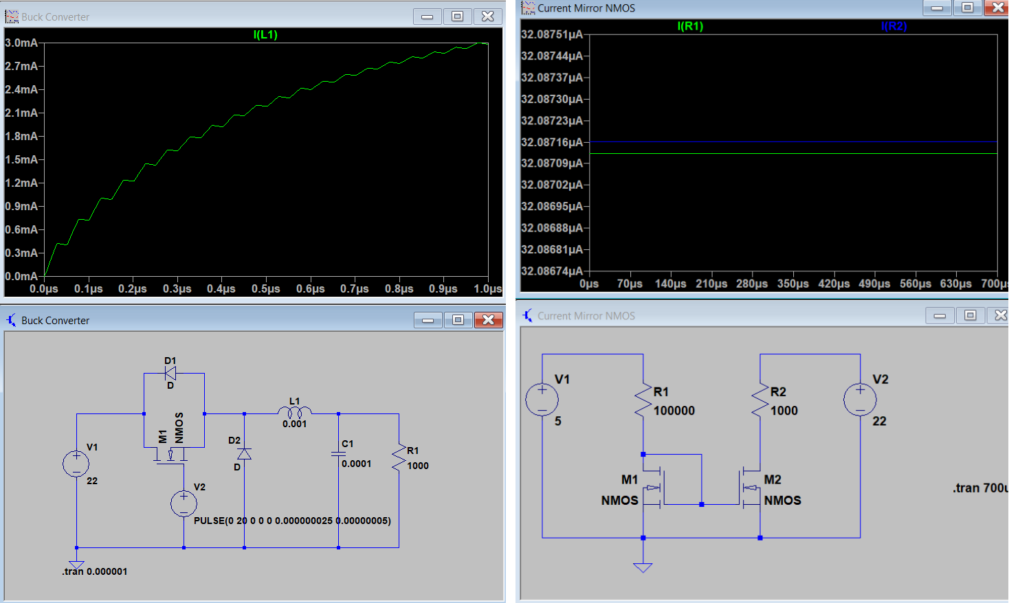
LTSpice and Current Control
I began to revise the hardware diagram created during week 3, as displayed above. The use of an op amp in series with an array of MOSFETS seemed particularly precarious.
To better understand how various circuit designs I was creating might perform, I started learning how to use LTSpice to perform transient analysis on circuit designs. This was initially a very daunting task for me, as I have no knowledge of LTSpice and very limited experience with circuit design. However, after going through various LTSpice tutorials and reading up on various electrical engineering principles, I now find this phase of the project to be much more enjoyable!
The primary challenge with the external PCB was to design a system which could handle various voltage and current requirements of a wide variety of programmable chips. I created various potential designs, including the use of a buck converter and an NMOS current converter. [depicted below]
The greatest epiphany came when I realized that designing such a circuit is challenging mostly because the internal resistance of the programmable chips will often not be known. Therefore, I am becoming increasingly convinced that a more workable approach is to design a circuit with current and voltage sensing to initially calibrate the circuit to a given chip model. Once the internal resistance of the chip has been determined, the FPGA will thereafter know how to properly provide the voltages and currents required for that particular model of programmable chip.
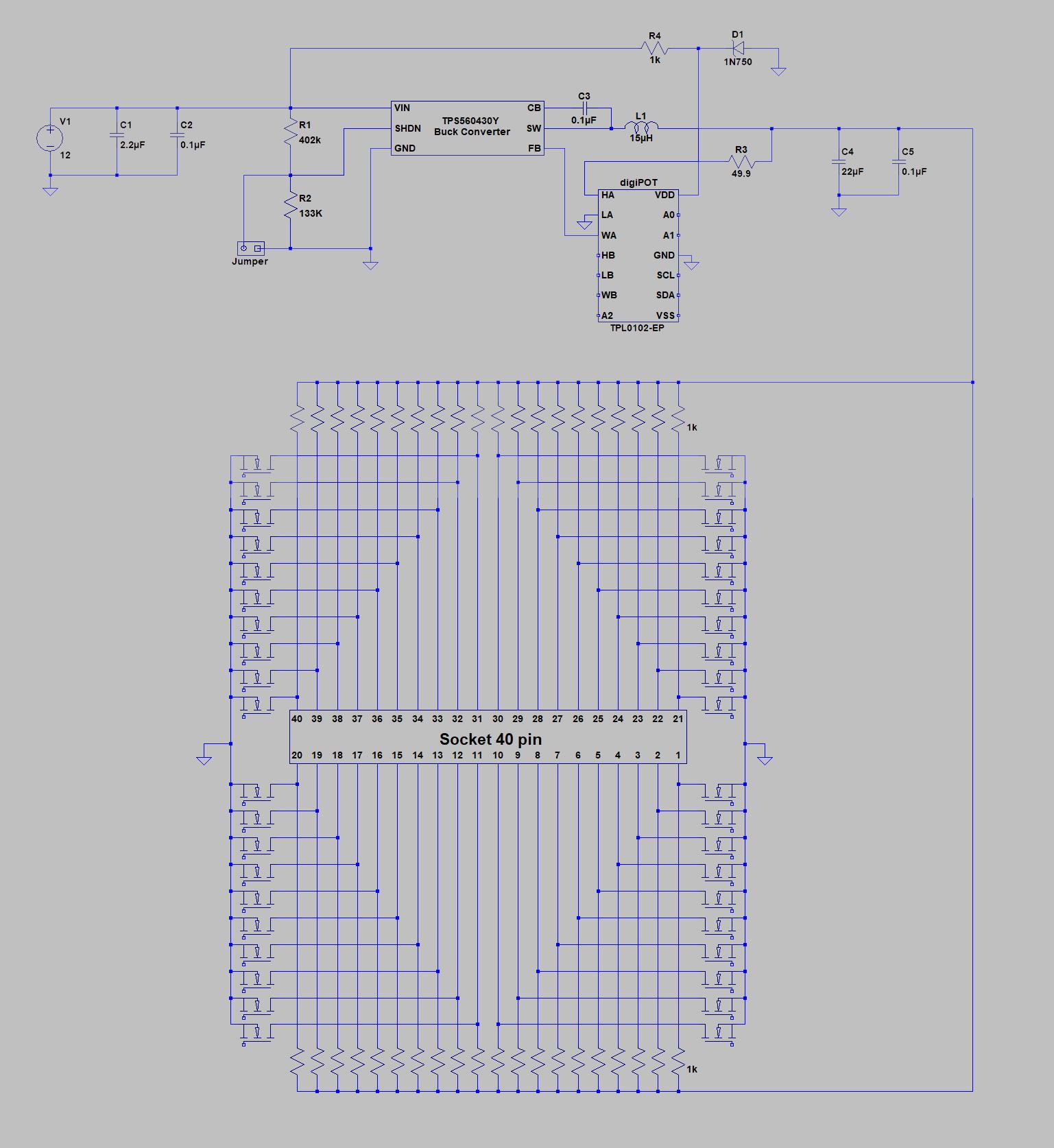
Circuit Near Completion
Circuit design is entirely new to me, though I have managed to complete the first draft of the circuit design. It is now capable of producing a voltage between 1 to 22 Volts using a buck converter controlled by a digital potentiometer.
I created the circuit schematic in LTSpice. Several of the chips in the design are not part of the native LTspice symbol library. I found that the Texas Instruments (TI) chips have PSPICE models. Alas, I was unable to get the TI models working in PSPICE. I then tried Tina-TI, also with no luck compiling the SPICE files for the TI parts.
In the end, I realized that the best approach is to instead create custom symbols in LTSpice for the TI parts. This was a time-consuming process, but I am quite happy with the end result.
The Intersection of Hardware and Software
With the first draft of the circuit complete, I focused my attention to the software aspects of the project. The FPGA will be sending signals from its GPIO pins to the custom PCB, where the programmable chip will be mounted. The challenge this week therefore became to determine how the FPGA will be programmed to perform specific read and write tasks with programmable chips.
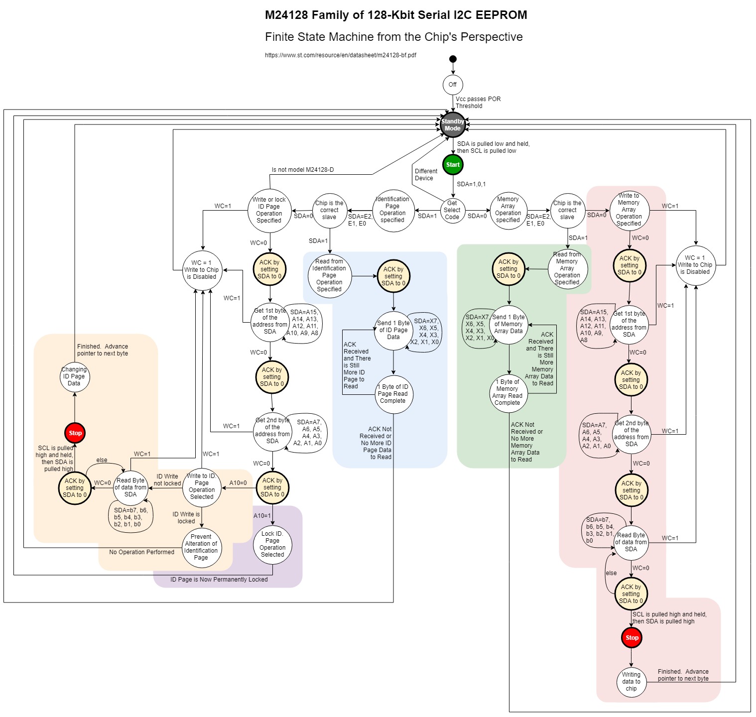
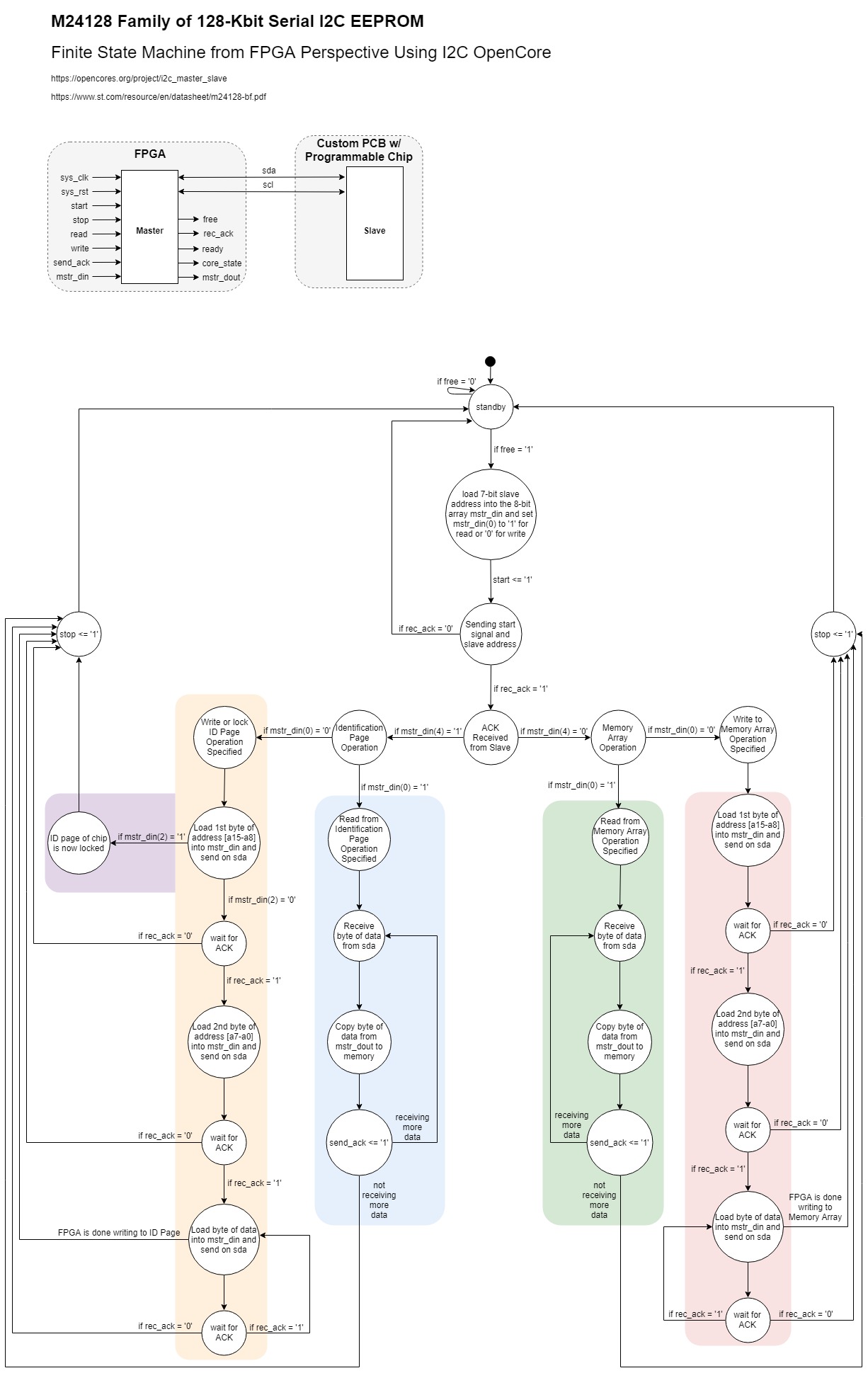
As an example of a commonly used type of programmable chip, a family of serial I2C EEPROM chips were chosen. After studying the functionalities of these types of chips quite thoroughly, I created a Finite State Machine (FSM) to represent the various logic states of the M24128 Family of 128-Kbit serial I2C EEPROM chips. The resulting FSM is depicted in the figure below.
After producing this FSM I learned that it is not necessary to implement the I2C portions of the FSM from scratch. Instead, an open-source IP core for serial I2C from OpenCores can be used. This would simplify the design process for the VHDL.
Choosing an Open-Source IP Core
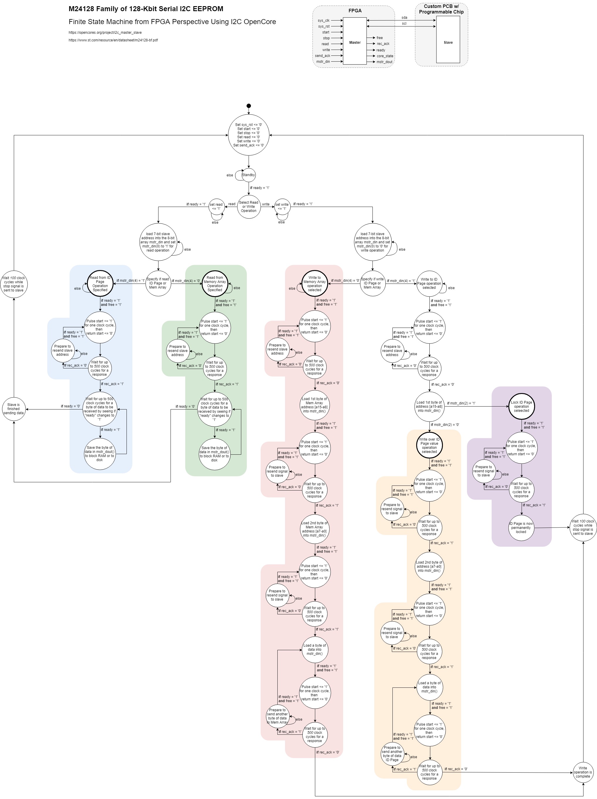
Last week's work resulted in the detailed Finite State Machine (FSM) depicted above. However, I realized that the FSM was created from the perspective of the programmable chip, and not the FPGA which would be performing the programming operation. While last week's FSM may prove quite useful for better understanding the M24128 family of Serial I2C EEPROM chips, it became apparent to me that I needed to create a new FSM which would help me to better understand how to use to the FPGA to interact with the programmable chips.
After spending quite a bit of time attempting to design my own implementation of I2C, I learned that there are open-source bits of VHDL code called Intellectual Property (IP) Cores, which are readily available for people to use in their own projects. Two of the PhD students from the lab identified an IP Core which implements I2C from the perspective of a master device. It was a bit tricky for me to understand, since the IP core does not have any documentation and only a few comments within the VHDL code. However, I knew that this could potentially save quite a bit of time, as opposed to designing my own implementation of I2C and attempting to debug it.
By the end of the week I had produced a new FSM, this time would represent the perspective of the FPGA which would be performing the read and write operations on the programmable chips.
Learning VHDL and Exploring Quartus Prime
Creating the Finite State Machine (FSM) last week taught me quite a bit, though my mentors have pointed out a few errors within it. So this week, I set about to redo the FSM to correct the errors.
The updated FSM is depicted below. It fixed many of the errors within the previous FSM, though I have learned that this too may not be entirely correct. Even so, I wanted to move on to work on a few more things before the week ended, including learning more about Quartus Prime, the Intel software used to interact with the Cyclone V FPGA.
Wrapping Everything Up
With my time in the Distributed Research Experiences for Undergraduates (DREU) drawing to an end, I began wrapping up the project. The work proved to be exceedingly challenging, though I had learned a great deal throughout these past many weeks.
The IoT Interface project will continue to be developed by fellow members of the Security in Silicon Lab (SSL). To summarize my progress on the IoT Interface project, I have created a formal paper, which can be downloaded here: IoT_Paper.pdf
Cheers,
Jacob Hazelbaker
Future Plans
The IoT Interface Project is still under development, though some additional features might be added in the future. Many of these features are things which I think would be great to have to ensure that a chip, once programmed, has not thereafter been tampered with.
- Return hash of the data currently on the chip
- Generate a unique value from speed at which electricity travels through the specific wires used to program the chip, since different wire lengths could produce slightly different electron travel times
- Investigate if it is possible to determine on some chips how many times they have been written to